|
GHOPTO
|
SWIR Cameras and Accessories in Semiconductor Inspection
| Price: | 100.0 USD |
| Payment Terms: | T/T |
| Place of Origin: | Shanxi, China (Mainland) |
|
|
|
| Add to My Favorites | |
| HiSupplier Escrow |
Product Detail
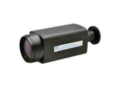
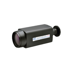
F25-300 F2.8-32 Zoom SWIR Lens
In the semiconductor inspection equipment, SWIR cameras can be used to inspect the quality of pure semiconductor material (usually silicon) after ingot growth. Furthermore, ingots that are subsequently sliced into wafers and these wafers can in a similar way be inspected for defects or cracks.
As the wafers are processed with successive layers to make transistors and memory cells used in modern integrated circuits, SWIR cameras are used to check alignment of the layers. High resolution scans of complete wafers are often accomplished with line scan cameras at the wafer defect inspection stage.
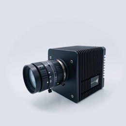
GHOPTO is a professional image sensor companies, we provide ingaas line scan camera, wafer inspection systems, 12k line scan camera, 3d line scan camera, high speed line scan camera, swir line scan camera, usb line scan camera, swir sensors, SWIR Cameras, SWIR Lenses & Accessories and etc. Want to know swir infrared? Please contact us.
Related Search
Find more related products in following catalogs on Hisupplier.com
Company Info
GHOPTO [China (Mainland)]
Business Type:Manufacturer
City: Taiyuan
Province/State: Shanxi
Country/Region: China (Mainland)